WaferEtch Wet Processing Platform
The WaferEtch platform is the industry choice for a number of critical aqueous-based processes in the advanced packaging, MEMs, RF, Data Storage and Photonics markets. There are 2 versions- the Manual Load (ML) and 3300 series platforms. The ML system is well suited for R&D and pilot environments. The 3300 series platform is the high volume work horse of the industry.The 3300 series architecture is extremely flexible as the user can have up to 8 chambers per system depending on throughput requirements. In addition, the system is capable of handling multiple wafer sizes and wafer types with minimal hardware modification. Lastly, the process chambers can be stacked vertically leading to extremely low system footprint.The Etch process chambers give a number of process control advantages versus wet bench and other single wafer alternatives.
주요 특징
- WaferChek Endpoint – Optical endpoint enables accurate identification of etch endpoint to minimize undercut, improve throughput, and lower chemistry cost.
- Hyperbolic arm scan control- User can tailor the dispense arm pattern to optimize etch uniformity
- Adaptive Spiking- Chemical concentration control to ensure stable etch rate batch to batch and within batch.
System Architecture
High Volume Platform- 3300 series
- 1 – 10 chamber modular system
- Low foot print- stacked chambers
- On board chemical supply
- Multiple wafer sizes- 50 to 300mm
- Multiple substrate types – Si, LiTaO3, Sapphire, Glass
Manual load platform for R&D- ML
- Single chamber- manual load

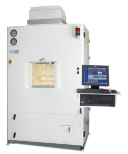
WaferEtch 3300 Series Platform Manual Load Platform
응용 분야
UBM/RDL Etch
- As I/O counts increase and performance requirements become more stringent, the RDL line/space dimensions continue to shrink. To enable these smaller dimensions, superior process control is required. The WaferEtch platform meets these process requirements with WaferChek endpoint and hyperbolic dispense arm motion.
Compound Semiconductor Etch and Silicon Thinning
- As the photonics and power markets continues to grow, manufacturers are scaling up their processes from bench scale to high volume. The WaferEtch system gives users the process control that bench scale approaches cannot, while also providing the wafer size and substrate flexibility.